Columnar crystalline silicon | Si material for semiconductor devices

Achieving both interposer-free and large-scale compatibility, while solving processing and process challenges of Si materials.
Do you have concerns about the design and manufacturing of semiconductor device components that need to accommodate large and complex shapes while also reducing chipping and cracking during processing? Our columnar crystalline silicon is a material characterized by being free of inclusions, high strength, and a unique crystal structure. It has processability and plasma etching characteristics equivalent to single crystal silicon, contributing to the reduction of processing defects and material-related issues. Additionally, we can accommodate round shapes up to a maximum diameter of 700mm and square shapes up to a maximum size of 1200mm, supporting greater design flexibility for large and complex shaped components. Furthermore, with a purity of 6N and being free of inclusions, we can expect a reduction in risks of abnormal discharge, particles, and metal contamination. This contributes to improved processing yield, increased equipment operating rates, and reduced maintenance burdens. We support the development of various silicon parts for plasma etching equipment, including retaining rings, susceptors, and transport hands. For more details, please check the Mitsubishi Materials official website and consult us through the inquiry form.
Inquire About This Product
basic information
- Contributes to reducing processing defects and abnormal discharge risks through the absence of interstitial materials. - Achieves processing characteristics and plasma etching properties equivalent to single crystal silicon. - High strength and excellent thermal properties. - Capable of handling round shapes up to a maximum diameter of 700mm and square shapes up to a maximum of 1,200mm. - Supports slicing, grinding, lapping, polishing, and etching processes. - S grade is a high-purity specification with a purity of 6N or higher but less than 7N. - Capable of processing to specified dimensions and shapes.
Price information
Please contact us through the official Mitsubishi Materials website.
Delivery Time
※The delivery time varies depending on the quantity, so please contact us through the Mitsubishi Materials official website.
Applications/Examples of results
■Components for Plasma Etching Equipment - Reduction of the risk of equipment shutdown due to abnormal discharge - Contribution to quality stabilization - Improvement of process stability - Increased yield through reduction of processing defects - Contribution to the improvement of component lifespan - Reduction of introduction burden by utilizing existing equipment and processes ■Susceptors, heat distribution plates, sputtering target materials, etc. - Increased design flexibility for large components - Expanded procurement options - Enhanced proposal capabilities for new equipment
Detailed information
-
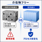
●Intermediary-free
-
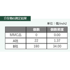
●Intermediary comparison data
-
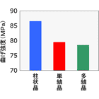
High strength and uniform crystal grain structure (bending strength)
-
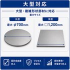
Supports up to large sizes.
-
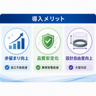
●Benefits of Implementation ・Reduction of processing defects ・Reduction of abnormal discharge ・Improvement of design flexibility
Company information

Advanced Products Division provides a wide range of high-performance materials and devices to customers worldwide. Our product portfolio includes semiconductor-related materials such as low-alpha solder and anti-reflective coatings for photoresists, as well as other high-quality products for precision assembly applications. In the field of environmental technologies, we are also driving the development of innovative and practical products that contribute to the realization of a sustainable next-generation society. Our portfolio includes infrared heat-shielding coatings for automotive and architectural applications, temperature sensors that enhance the performance and safety of electric vehicles (xEV), and lightning protection components that improve the reliability of social infrastructure. Furthermore, our advanced assembly materials, featuring high heat resistance, low electrical resistance, and excellent thermal conductivity, have earned strong recognition both in Japan and overseas. These products are expected to serve as key drivers of our future growth.


![[Case Study] Sensor Reduces Sorting Time by Half! Higashi Nihon Recycling Systems](https://image.www.ipros.com/public/product/image/add/2001211187/IPROS42997668617422795954.png?w=280&h=280)
![[Case Study] 90% Recycling Rate of Waste Plastics! Meiwa Packs](https://image.www.ipros.com/public/product/image/c34/2001211193/IPROS77251652406533655175.png?w=280&h=280)