Wafer can be evaluated using photoluminescence during the solar cell manufacturing process.
The PVX1000+POPLI-Octa can evaluate wafers during the solar cell manufacturing process using photoluminescence. It is capable of assessing the passivation effects of the PN junction layer after thermal diffusion, the AR layer deposition, surface contamination, as well as the protective effects of the rear insulation layer and the evaluation of Local-BSF. Additionally, by using a DC power supply for EL observation of the module, it is possible to pinpoint the locations of defects. By applying reverse bias to the module and observing LEAK points, defects that have caused PID can be easily identified.

Inquire About This Product
basic information
Product Features 1. Silicon wafers (6 inches or smaller) 2. Ultra-high sensitivity cooled CCD camera (1 million pixels, -70°C) 3. Bulk imaging measurement possible with surface light source 4. Equipped with high-function image processing software 5. Compact tabletop design
Price range
Delivery Time
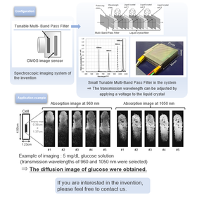
Applications/Examples of results
We can conduct a demo using customer samples. We also accept customizations based on individual requests. Please feel free to contact us here.
catalog(1)
Download All Catalogs
Company information

Aites was established in 1993, originating from the quality assurance department of the IBM Japan Yasu office. Based on the technical expertise cultivated through cutting-edge defect analysis and reliability assurance of electronic components at the IBM Japan Yasu office, we have provided various products and services that support the development and manufacturing of semiconductors, displays, organic EL, solar cells, and electronic components to customers both domestically and internationally.