Infrared imaging and spectroscopic measurements are possible, achieving a spatial resolution of 10 nm.
The nano-FTIR【neaSCOPE】 manufactured by attocube systems is a Fourier transform infrared spectrometer that performs spectral imaging and spectral measurements with a resolution of up to 10 nm. Using patented technology, it extracts only the infrared spectrum from scattered light, achieving a spatial resolution of 10 nm. The excitation wavelengths range from visible to terahertz, supporting further exploration in material science. It is ideal for various fields that require higher spatial resolution, including scientific disciplines, semiconductor technology, polymer chemistry, and life sciences. 【Features】 ■ Patented background noise removal technology from attocube systems ■ Achieves imaging and spectral measurements with high spatial resolution of 10 nm ■ Developed a dedicated AFM that enables high reproducibility and high-sensitivity detection ■ Allows measurement of bulk cross-sections with sample preparation suitable for AFM measurements ■ No need for sample thinning! For more details, please contact us.

Inquire About This Product
basic information
【Specifications】 ○ Scan area: 100×100μm (closed loop) ○ Sample stage ・Motor drive: Maximum travel range X=60mm, Y=15mm, Z=6mm (AFMs head side X=30mm, Y=3mm, Z=4mm) ○ Noise level: <0.2nm RMS (1.5 - 150Hz) ○ Optical microscope ・Horizontal resolution 0.8μm, field of view 0.7mm ・Long working distance objective lens (WD=20mm) ○ CCD camera: 5Mpix high-speed digital imaging ○ Excitation wavelength ・Visible, infrared, and terahertz (400nm–200µm) * Nano-spectroscopy in the mid-infrared range is possible with a dedicated broadband light source. ● For more details, please contact us.
Price range
Delivery Time
Applications/Examples of results
【Usage】 ○ As a Fourier Transform Infrared Spectrometer → Imaging and spectral measurement are possible ● For more details, please contact us.
Detailed information
-
![IPROS4043543862333322558_140x140[1].jpg](https://image.www.ipros.com/public/product/image_diagram/da6/462473/IPROS32198825473611175110.jpeg?w=140&h=140)
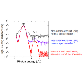
PMMA/PS polymer blend Imaging focused on the PMMA structure at a wavenumber of 1740 cm-1. Both reflection and phase images were simultaneously obtained with AFM. The signal-to-noise ratio was measured well, allowing for the visualization of compositional information down to fine structures.
-
![IPROS5878912403747856132_140x140[1].jpg](https://image.www.ipros.com/public/product/image_diagram/4e3/462474/IPROS91307482660275473933.jpeg?w=140&h=140)
Organic foreign matter The main component of the foreign matter attached to the PMMA substrate is PDMS, and high spatial resolution fingerprint region spectra were obtained without the influence of the substrate. Additionally, when performing line spectrum mapping (30 points at 20 nm steps) across the PMMA/silicon interface on the same sample, peaks originating from PMMA disappeared in one step near the interface, confirming high spatial resolution not only in fixed wavenumber imaging but also in spectroscopy.
-
![IPROS2521825921598308528_140x140[1].jpg](https://image.www.ipros.com/public/product/image_diagram/873/462475/IPROS28286778184124280722.jpeg?w=140&h=140)
Defects on SiC In the compound semiconductor SiC, intrinsic defects that are not visible in AFM images around the indentation are visualized with high resolution.
-
![IPROS5307791661177340588_140x140[1].jpg](https://image.www.ipros.com/public/product/image_diagram/9a0/462476/IPROS71995520223299683873.jpeg?w=140&h=140)
CVD graphene film Visualization of electrical and plasmonic phenomena at CVD graphene grain boundaries using scanning plasmon interference method. Grain boundaries that are not clearly visible in the topography images obtained by AFM are distinctly indicated by the standing waves due to plasmon scattering.
-
![IPROS5277086068192749737_140x140[1].jpg](https://image.www.ipros.com/public/product/image_diagram/44d/462477/IPROS45408884180318716666.jpeg?w=140&h=140)
Organic semiconductor (pentacene) crystal phases A pentacene film approximately 40 nm thick was deposited on SiO/Si using thermal deposition, and terraces were confirmed from the surface roughness image (diameter about 3 mm, height about 1.5 nm). Near-field spectroscopy allows for the identification of each crystal phase, which has been verified by XRD and other methods. Spectra were measured by separating two points approximately 1 µm apart. Differences of just a few cm⁻¹ can be detected. Understanding the crystal phases is important because the macroscopic conduction properties of pentacene are determined by the nanoscale domain structure.
catalog(1)
Download All Catalogs
Company information

Our company was established as the Japanese subsidiary of a foreign-affiliated manufacturer with a global network spanning over 40 countries. We are steadily expanding our business primarily through the sale of SQUID magnetic property measurement devices and physical property measurement devices, which boast a world-class market share in the field of new material research and development. Additionally, we also function as a trading company for high-tech scientific instruments, importing and selling cutting-edge research equipment from around the world in various fields such as material science, biotechnology, and nanotechnology. The wave of technological innovation is transforming not only industrial sectors but also our daily lives. Among these, the fields of material science, biotechnology, and nanotechnology, which are the pillars of our business, can be described as "core technologies" that provide humanity with infinite possibilities for the future as they drive cutting-edge technology (high-tech). Discoveries such as high-temperature superconducting materials, applications of laser microfabrication and optical communication, and surface analysis at the nanoscale play crucial roles in various fields including new materials, semiconductors, information and communication, medical care, clinical diagnostics, and drug discovery, while also enabling further advancements in technology.